About Silicon
Silicon, Si:
The most common semiconductor, atomic number 14, energy gap Eg= 1.12 eV- indirect bandgap; crystal structure- diamond, lattice constant 0.543 nm, atomic concentration 5 x 10²² atoms/cm-3, index of refraction 3.42, density 2.33 g/cm3, dielectric constant 11.7, intrinsic carrier concentration 1.02 x 1010 cm-3, mobility of electrons and holes at 300°K: 1450 and 500 cm2/V-s, thermal conductivity 1.31 W/cm°C, thermal expansion coefficient 2.6 x 10⁻⁶°C-1, melting point 1414°C; excellent mechanical properties (MEMS applications); single crystal Si can be processed into wafers up to 300mm in diameter.
P type= Always Boron (B) Doped
N type= Dopant typically as follows:
Res: .001-.005 Arsenic (As)
Res: .005-.025 Antimony (Sb)
Res: >.1 Phosphorous (P)
Wafer Flats:
Purpose and Function
- Orientation for automatic equipment
- Indicate type and orientation of crystal
Primary Flat = The flat of longest length located in the circumference of the wafer. The primary flat has a specified crystal orientation relative to the wafer surface; major flat.
Secondary Flat = Indicates the crystal orientation and doping of the wafer. The location of this flat varies.
P type <111> No secondary Flat
P type <100> 90°�5° Clockwise from Primary Flat
N type <111> 45°�5° Clockwise from Primary Flat
N type <100> 180°�5° Clockwise from Primary Flat
Cleaving:
- Using a diamond scribe
- Cleaves will run according to the following crystal orientations for Silicon:
- If the crystal orientation of the Si is <100> the cleaved pieces form rectangles (cleave at 90 deg. angles).

- If the crystal orientation of the Si is <111> the cleaved pieces form triangles (cleave at 60 deg. angles). <111> material has triangular crystal structure. You have to scribe up through the base of the triangle, as opposed to the vertex of the triangle, so orientation is important. Usually, this is delineated by a flat along the 110 plane. Cleaving samples on <111> wafers for SEM imaging can be difficult.

Crystal Planes in Semiconductors
Miller Indices:
All lattice planes and lattice directions are described by mathematical description known as a Miller Index. This allows the specification, investigation, and discussion of specific planes and directions of a crystal. In the cubic lattice system, the direction [hkl] defines a vector direction normal to surface of a particular plane or facet. The Miller Indices h,k,l are defined as follows:
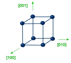 |
type: <100> Equivalent directions: [100],[010],[001] |
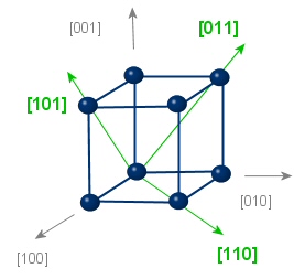 |
type: <110> Equivalent directions: [110],[011],[101], [-1-10],[0-1-1],[-10-1], [-110],[0-11],[-101], [1-10],[01-1],[10-1] |
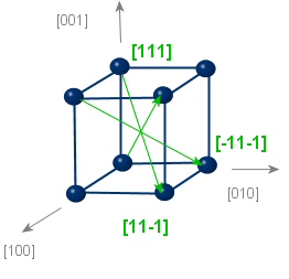 |
type: <111> Equivalent directions: [111],[-111],[1-11],[11-1] |
- Silicon on Insulator (SOI):
- Only a thin layer on the surface of a silicon wafer is used for making electronic components; the rest serves essentially as a mechanical support. The role of SOI is to electronically insulate a fine layer of monocrystalline silicon from the rest of the silicon wafer. Integrated circuits can then be fabricated on the top layer of the SOI wafers using the same processes as would be used on plain silicon wafers. The embedded layer of insulation enables the SOI-based chips to function at significantly higher speeds while reducing electrical losses. The result is an increase in performance and a reduction in power consumption. There are two types of SOI wafers. Thin film SOI wafers have a device layer <1.5 �m and thick film wafers have a device layer >1.5 �m.
- Wafer bonding. - In this process the surface of two wafers are coated with an insulating layer (usually oxide). The insulating layers are then bonded together in a furnace creating one single wafer with a buried oxide layer (BOX) sandwiched between layers of semiconductor. The top of the wafer is then lapped and polished until a desired thickness of semiconductor above the BOX is achieved.
- SIMOX - Seperation by Implantation of Oxide. In this process a bulk semiconductor wafer is bombarded with oxygen ions, crating a layer of buried oxide. The thickness of intrinsic semiconducor above the box is determined by the ion energy. An anneal reinforces Si-O bonds in the BOX.
- Smart Cut - The wafer bonding method is used to form the BOX, but instead of lapping off excess semiconducor (which is wasteful) a layer of hydrogen is implanted to a depth specifying the desired active layer of semiconductor. An anneal at ~500°C splits the wafer along the stress plane created by the implanted hydrogen. The split wafer may then be reused to form other SiO wafers.
- III-V Semiconductors:
- Gallium Arsenide, GaAs - After silicon, the second most common semiconductor, energy gap Eg = 1.43 eV, direct bandgap; crystal structure - zinc blend, lattice constant 5.65 Ang., index of refraction 3.3, density 5.32 g/cm3, dielectric constant 12.9, intrinsic carrier concentration 2.1 x 106 cm-3, mobility of electrons and holes at 300°K - 8500 and 400 cm2/V-s, thermal conductivity 0.46 W/cm°C, thermal expansion coefficient 6.86 x 10⁻⁶ °C-1; thermally unstable above 600°C due to As evaporation; does not form sufficient quality native oxide; mechanically fragile; due to direct bandgap commonly used to fabricate light emitting devices; due to higher electron and hole mobilities, also foundation of the variety of high-speed electronic devices; bandgap can be readily engineered by forming ternary compounds based on GaAs, e.g. AlGaAs.
- Gallium Nitride, GaN - wide bandgap III-V semiconductor withdirect bandgap 3.5 eV wide; among very few semiconductors capable of generating blue radiation, GaN is used for blue LEDs and lasers; intrinsically n-type semiconductor but can be doped p-type; GaN is formed as an epitaxial layer; Lattice mismatch remains a problem, creating a high defect density. Incorporation of Indium (InxGa1-xN) allows control of emission from green to violet (high and low In content respectively). GaN can also be used in UV detectors that do not respond to visible light. GaN has a Wurtzite(W) or Zinc Blend(ZB) crystal structure. Lattice constant [A] 3.189(W) 5.186(ZB); Density[g/cm3] 6.15(W) 6.15(ZB); Atomic concentration [cm-3] 8.9 x 10²²(W) 8.9 x 10²²(ZB); Melting point [°C] 2,500(W) 2,500(ZB); Thermal conduct.[W/cm °C] 1.3(W) 1.3(W); Thermal expansion coefficient[°C-1] ~1x10⁻⁶; Dielectric constant (static) 8.9(W) 9.7(ZB); Refractive index 2.4(W) 2.3(ZB);
- GaP - Crystal structure zinc blend; Lattice constant [A] 5.45; Density [g/cm3] 4.14; Atomic concentration [cm-3] 4.94 x 10²²; Melting point [°C] 1457; Thermal conductivity [W/cm °C] 1.1; Thermal expansion coefficient[1/°C] 4.65x10⁻⁶; Dielectric constant 11.1; Refractive index 3.02; Energy gap [eV] 2.26; Type of energy gap: direct; Electron mobility [cm2/V sec] 250; Hole mobility [cm2/V sec] 150;
Print This Page
NOVA offers the best competitive pricing without sacrificing quality. No order is too big or too small for us to handle. Contact Us today.