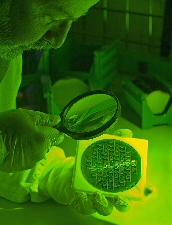
Wafer Services
NOVA is a valuable resource for our clients’ confidential customized needs because we partner with industry-recognized, experienced suppliers to ensure you receive the highest quality wafer processing services. NOVA has a large selection of prime and test grade silicon wafers available in diameters of 1” to 12” to accommodate your processing needs. Services can also be performed on customer supplied material.
You can count on NOVA to provide exceptional customer service, quality processing with quick turnaround, at affordable pricing. Contact us today to discuss your wafer processing requirements.
Processing services include:
Thin Films – A wide variety of custom films to satisfy MOS/MEMS process requirements
Metal Deposition – Sputtered PVD Metals and Dielectrics as well as E-Beam Evaporation process
Wafer Processing – Full range of wafer processing services for MEMS and Micro-Machining projects
Wafer Reclaim/Recycle – Full wafer recovery extending the lifecycle of a wafer as well as a cost effective solution for our customers
Contact NOVA for more information on our processing services at (972)478-7002 or submit an online Service Request.
Print This Page
NOVA offers the best competitive pricing without sacrificing quality. No order is too big or too small for us to handle. Contact Us today.